Build Log — Custom Flight Controller

Designing a flight controller, and everything that went wrong on the way

An STM32F405 flight controller for a 4S freestyle quad, running Betaflight off a target I wrote. I started it to find out whether I could take an embedded system from a blank schematic to something that actually flies.

I've been keeping this log since May, and I've kept the entries that make me look bad. A gyro that stopped existing mid-design, a flash chip a quarter the size I ordered, and a DMA collision that read as a hardware fault for a full day. Those are the interesting parts.

Last update
StatusBench bring-up, not flying
Entries10
Bench test

One motor, full throttle, nothing caught fire

Pack and USB live at the same time, throttle up, and it just ran. The blackbox flash, on the other hand, is dead.

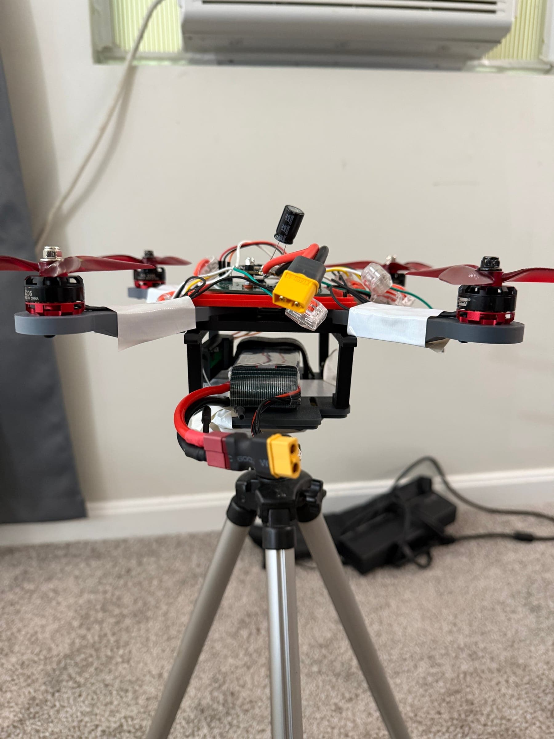
Throttle up on the FlySky, board powered from the pack and USB at once.

Spun a motor off the board today. LiPo in through CN1, USB-C plugged in at the same time, throttle up, and it just ran. Clean. No stutter, no brownout, no smoke.

The dual-source part is what I actually cared about. Three ORing diodes (D3, D4, D7) sit between the buck's 5 V and USB's 5 V, and until today I had never had both live at once. If I'd gotten those backwards I'd have found out by watching one source shove current into the other. Instead nothing happened, which is the correct outcome and a deeply boring thing to celebrate.

Receiver is bound. i-BUS into UART1, live channel data in the Configurator. Current sense on PA2 reads correctly with the motor under load.

The blackbox flash is dead. Not miswired. Dead. I went back and re-checked every pin by hand: VCC, /HOLD, /WP, /CS, all four SPI2 continuity points, pin-1 orientation, no MISO-to-ground short (1.4 MΩ). Every one of them is exactly what it should be, and flash_info still comes back with nothing.

Betaflight CLI
# flash_info
Flash sectors=0, sectorSize=0, pagesPerSector=0, pageSize=0, totalSize=0 JEDEC ID=0x00000000

All zeros rather than all ones is the tell. An open MISO floats high and reads 0xFFFFFF. Reading 0x000000 means the MCU clocked out the read command and watched the data line sit low the whole time. The chip never answered. Nothing left to blame but the die. I have five spares, so it's a hot-air swap, with the nozzle kept narrow and well away from U7. The BMI270 is the one part on this board I don't want to reflow twice.

Still open: three motors have not been spun individually, and failsafe hasn't been tested at all. It doesn't fly yet.

Bring-up

It runs, and an ADC bug ate a day

Staged bring-up through the solder jumpers, one rail at a time. Everything passed except the two ADC channels I needed most.

Bring-up went stage by stage through the solder jumpers, the way the board was designed to be brought up. Nothing behind a closed jumper could take out anything ahead of it. That design decision earned itself back today.

  • 3.3 V rail up, MCU running, enumerated over USB as STM32 BOOTLOADER (0483:DF11).
  • Clock=168MHz (PLLP-HSE) in status, so the 8 MHz crystal and its load caps are good.
  • Vref=3.28V, which is only readable if VDDA is live, so the FB1 wire link works.
  • TPS5450 buck put out 4.98 V from a 15.58 V pack. 0.4% off target.
  • Bridged JP10 and the gyro appeared immediately: GYRO=BMI270, ACC=BMI270, GYRO rate: 3225.
  • Four DShot outputs landed on DMA1 streams 7, 2, 6 and 1. Four distinct streams, no clash.

That last one closes out the motor remap I did back in June. The pin I moved to dodge a DMA collision actually stayed clear on real silicon.

Then I lost a day to the ADC.

status was showing a healthy Vref=3.28V and a core temperature climbing normally. Directly underneath it: Voltage: 0 * 0.01V (0S battery - NOT PRESENT). Meanwhile my meter read 1.4 V on PA1. Divider verified. JP8 verified. battery_meter = ADC, adc_device = 1, resource mapping correct. Everything downstream of that pin measured perfect and the reading stayed at a hard zero.

On the F405, ADC1's regular-conversion DMA defaults to DMA2 Stream 0 Channel 0. SPI1_RX, which is the gyro, defaults to DMA2 Stream 0 Channel 3. Same stream. SPI1 gets allocated first and wins, and then the ADC driver does this:

betaflight/src/main/drivers/adc_stm32f4xx.c
if (!dmaAllocate(dmaGetIdentifier(adc.dmaResource), OWNER_ADC, 0)) {
    return;
}

It gives up silently. No error, no boot warning, no log line. The regular conversion sequence never runs and every external ADC channel reads zero forever. Battery voltage and current, both.

The reason it hides so well: on F4, Vref and core temperature come through injected channels triggered by software polling, which need no DMA at all. So the ADC looks completely healthy in status while the two channels you actually want are gone. You will blame the solder jumper, the divider, the resistors, the pin map and the chip itself long before you blame DMA.

Fix, now permanent in the target
#define ADC1_DMA_OPT 1      // ADC1 -> DMA2 Stream 4, clear of SPI1

Also trimmed vbat_scale from 110 to 111 to land the reading on the pack voltage, and corrected LED0_PIN to PC14 after the status LED refused to blink.

Assembly

Two resistor swaps that would have killed the board

Generated a placement guide from the KiCad file before any paste went down, organised by part value instead of by reference designator.

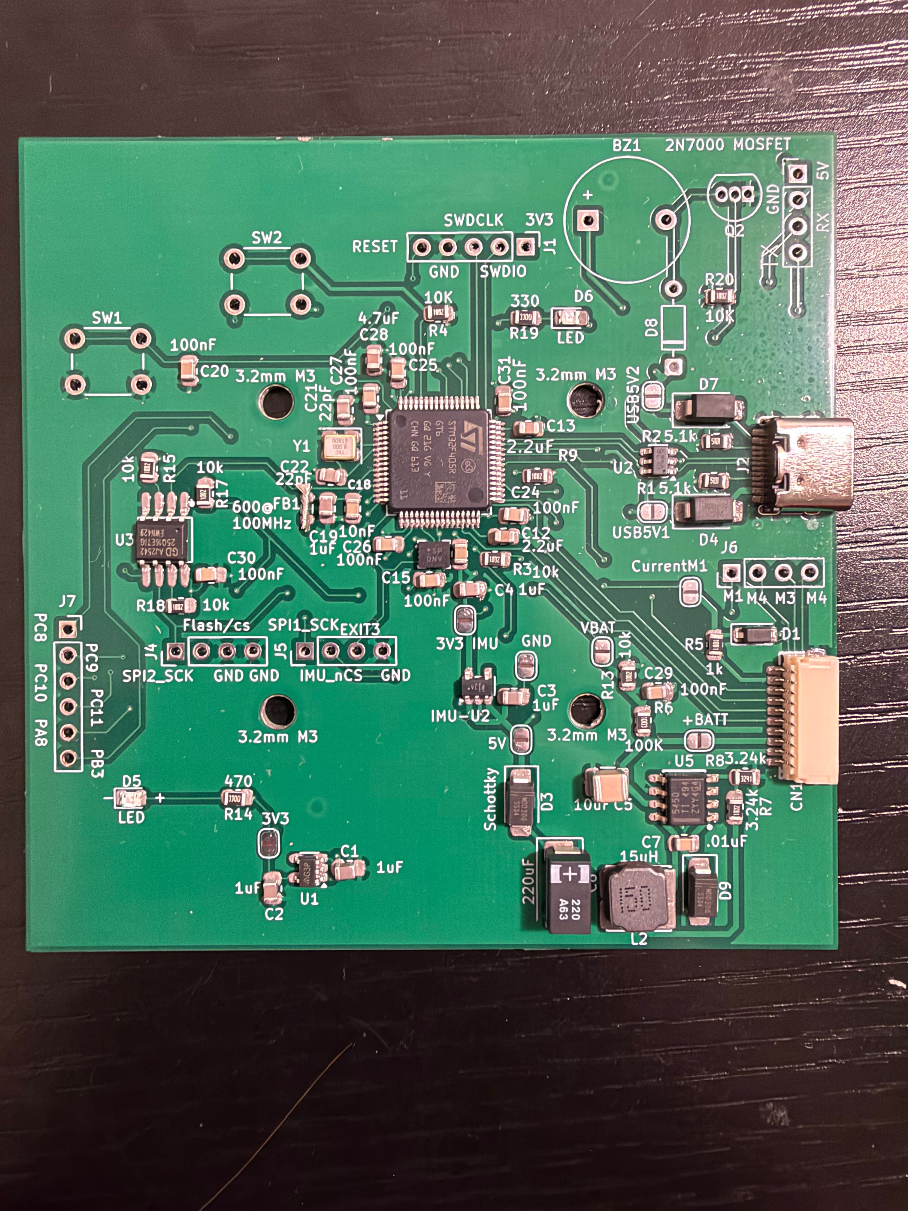
Assembled STM32F405 flight controller PCB after hotplate reflow
Everything placed, one reflow pass, no rework yet.

Before any paste went down I generated a placement guide straight out of the KiCad file, by reading actual pad-to-net connections rather than trusting the BOM. It is organised by part value, not by reference designator, because that's how you assemble: open one strip, place every position for that value, seal the strip, open the next. Never two strips out at once.

That sounds like a lot of ceremony for a board with sixty-odd passives. It isn't. Two pairs on this board are physically adjacent, identical at 0805, and silently wrong if swapped.

R6 (marked 1003, 100 kΩ) and R13 (1002, 10 kΩ) are the VBAT divider. Swapped, PA1 sees 15.3 V instead of 1.53 V and the pin dies the first time a pack goes in.

R7 (1002) and R8 (3241) set the buck feedback. Swapped, the converter outputs 1.221 × (1 + 3.24/10) = 1.62 V instead of 5 V. Nothing downstream runs and you spend an evening blaming the TPS5450.

One deliberate change from the BOM: R14 went from 470 Ω to 330 Ω. The 470 was sized for the red power LED I originally specified. The LEDs that actually turned up are green, Vf around 2.55 V, which left D5 at roughly 1.6 mA and basically invisible. At 330 Ω it runs about 2.3 mA. D6 keeps its own 330 Ω for a different reason: it hangs off PC14 in the backup domain, which is limited to about 3 mA.

Everything goes down value-side-up so I can read the markings back afterwards instead of taking my own word for it.

Sourcing

The IMU stopped existing, and the flash is a quarter the size I ordered

The entire ICM-426xx family went reel-only in one week. Then I found out I had ordered a 2 MB flash chip instead of a 16 MB one.

Two bad discoveries in one day.

The gyro first. I had designed around a TDK ICM-42605. Somewhere between choosing it and needing it, the whole 426xx family went reel-only at LCSC, minimum order a thousand-plus, and out of stock at DigiKey and Mouser. In quantity one it simply stopped existing.

The replacement is a Bosch BMI270. It shares the 2.5 × 3.0 mm LGA-14 outline and that is the entire extent of the similarity. Different pinout, so: new footprint, every IMU net re-routed, different decoupling (100 nF at VDD and 100 nF at VDDIO, where the 42605 wanted a 2.2 µF / 0.1 µF / 10 nF set), and the unused-pin strapping inverted. ASDx and ASCx now go to VDDIO and must not be grounded, which is exactly what the 42605's RESV pins wanted.

Here's the part I want to be honest about. The power tree absorbed all of it with zero changes. VDD stayed on the quiet TLV733P rail, VDDIO stayed on the main AP2112K rail. A forced sourcing change cost me a footprint and a re-route instead of a power redesign. I'd love to say I planned for that. I didn't. I split the rails back in June because I didn't want digital switching noise on the gyro supply, and it happened to pay off two months later for a completely unrelated reason.

The cost is real, though. The BMI270 ships uncalibrated, which is precisely why Betaflight discourages it for new designs, and it caps the PID loop at 3.2 kHz instead of 8 kHz. For Acro freestyle neither matters much. I took the downgrade because the alternative was not having a board.

Then, while reconciling three different BOM files against each other, I found the flash. U3 as ordered and fitted is a GigaDevice GD25Q16E: 16 Mbit, so 2 MB. The BOM called for a 128 Mbit part. The wrong one made it onto the order and I caught it a week after the boards shipped, which tells you plenty about how I was managing the BOM.

I'm keeping it. Betaflight identifies SPI NOR by JEDEC ID at runtime, and the GD25Q16E is already in the m25p16 driver's table, so nothing changes in firmware. Configurator reporting 2 MB is correct behaviour, not a fault.

betaflight/src/main/drivers/flash_m25p16.c
{ 0xC84015, 104, 50, 32, 256 }   // GigaDevice GD25Q16E
// 32 sectors x 256 pages x 256 B = 2,097,152 bytes

What I lose is log duration, not function. Roughly 22 seconds at 3.2 kHz, 44 at 1.6 kHz, 87 at 800 Hz. Tuning runs are 30 to 60 seconds anyway, and 800 Hz still resolves everything below 400 Hz, which is where the motor and frame noise peaks that filter tuning depends on actually live. The real loss is that I can't log a whole pack. Every candidate upgrade shares the same SOIC-8 208-mil footprint, so fixing it later is a hot-air swap.

Firmware

Writing firmware for a board that doesn't exist yet

Boards are somewhere between Shenzhen and here, so I wrote the Betaflight target and found out my own docs disagreed with my own schematic.

Nothing to solder yet, so I wrote the firmware target: betaflight_target/ETHANF405/config.h, plus a build and flash guide so future me doesn't have to re-derive the sequence.

Reconciling the pin map against the fabricated board turned up a problem. My planning docs and the actual schematic disagreed. The board is already made, so the schematic wins and the docs are wrong. Motors are PB0, PB1, PA3 and PB10 (TIM3_CH3/CH4, TIM2_CH4/CH3), not what the older notes claimed. Flash MISO is on PC2, not PB14. Current sense is PA2. The status LED hangs off the backup domain through 330 Ω, so it will be dim, and that's by design rather than a mistake I get to fix.

All of it went into one file, VERIFIED_PINOUT.md, which is now the only pin document I trust. The older tables got marked superseded rather than deleted, because I want to be able to see what I got wrong and when.

Also built a 5-inch frame while waiting. It's a Python script on top of trimesh that unions a centre plate, four arms and four motor pads, subtracts the hole pattern, and writes an STL. 220 mm wheelbase, 30.5 mm stack holes, 16 mm motor bolt pattern, with a thinned pocket under each motor pad. Parametric, so changing the wheelbase is one number. Printing it is a later problem.

Fab

Ordered. $130 and two weeks of not knowing

Bare 4-layer, ENIG, frameless stencil, quantity five.

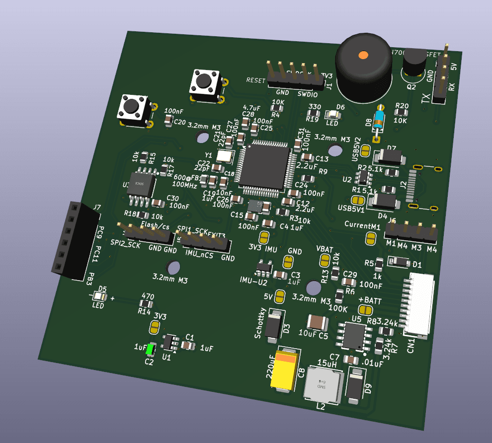
KiCad 3D render of the flight controller board, angled view
What I was hoping would show up in two weeks.

Sent it to JLCPCB. Bare 4-layer, ENIG finish, frameless top-side stencil, quantity five. The commit message I wrote that day was "Ordered the PCB now i have to wait and see if i waisted 130 dollars," which is an accurate record of the mood.

ENIG mostly for the LGA gyro and the fine-pitch parts. HASL is fine for through-hole and 0805. It's less fine for a package whose joints you can't inspect after the fact.

Two weeks out. Nothing to do but write firmware and worry about the two BOM questions I had not closed: whether the TPS5450 or the older TPS5430 actually shipped, and whether the buck inductor is the 15 µH the TI worked example calls for or the 22 µH left over from when this was a 6S design. Both get answered with a meter and a magnifier before anything gets populated.

Schematic

Schematic finished, checked pin by pin

Current-sense clamp, VBAT divider, SWD header, then a full netlist walk against the KiCad files.

Finished the last of the analog and debug circuitry.

A current-sense clamp on the ESC's current line: 1 kΩ in series with a 3.3 V zener to ground, ADC tapped between them. The ESC is under no obligation to keep that line inside 3.3 V and I'd rather not learn that the expensive way.

A VBAT divider, 100 kΩ over 10 kΩ with a 100 nF cap, so a 16.8 V full pack lands at 1.53 V. An SWD header, because if USB DFU refuses to cooperate I want a second way into the chip. A power-good LED on the main 3.3 V rail, and I removed the one I had put on the quiet IMU rail. No reason to hang a few milliamps of load on the supply I went out of my way to keep clean.

Then I walked the netlist pin by pin against the KiCad files: MCU core, all fourteen IMU pins, flash, USB and its ESD part, both LDOs, the ORing diodes, boot and reset, current sense, the VBAT divider, SWD. ERC clean.

Next: layout.

Design

6S to 4S, and a motor that had to move

Motor 4 wanted the same DMA stream as the blackbox flash. That is not a compile error, it is a bad afternoon.

Dropped the target battery from 6S to 4S. 14.8 V nominal, 16.8 V charged. That relaxes the input capacitor voltage rating and moves the buck's output inductor to 15 µH, which is what TI's worked example calls for at this input and output pair.

The more interesting change is that motor 4 had to move. It was sitting on a pin that wants DMA1 Stream 3, and so does SPI2_RX, which is the blackbox flash. DShot and the logger would have been fighting over the same stream. That failure doesn't show up as a compile error. It shows up as a motor misbehaving only while you are logging, which is the worst possible way to find a bug.

Remapped it and checked the new assignment against the DMA request tables in RM0090. I still don't fully trust the table. dma show all on real hardware is the check that counts, and that went on the bring-up list.

Architecture

The ESC has no BEC, so the board needs its own buck

The most useful constraint on this project turned out to be the one I set for myself.

The constraint I set myself: this has to mate with the ESC I already own, a Flycolor Raptor BLS-04 4-in-1, on its existing 10-pin SH1.0 harness.

That turned out to be the most useful decision on the project, because the BLS-04 has no BEC. It hands you raw pack voltage and nothing else. So the board carries its own buck converter running off up to 16.8 V, which is a far more interesting problem than accepting a regulated 5 V from somewhere else. The external Matek BEC I had planned for is gone.

Also locked today: 4-layer stackup, every SMD part on the top side so the whole board goes through one hotplate reflow pass, hot air for the LGA gyro. The board is oversized for the stack while keeping the standard 30.5 mm mounting pattern. On a real build that would be silly. I'm hand-placing every part, and the extra room is worth more to me than looking sensible.

Gyro stays the ICM-42605. I evaluated the BMI270 and rejected it, on the grounds that Betaflight discourages it for new designs. Worth remembering in July.

Kickoff

Starting

Take an embedded system from a blank schematic to something that flies, and don't skip the annoying parts.

The goal: take an embedded system from a blank schematic to something that flies, and don't skip the parts that are annoying.

STM32F405, because Betaflight supports it natively and writing a custom target is a good chunk of why I'm doing this at all. The first pass at the power architecture assumes an external Matek MBEC6S for 5 V and a 6S pack. Both of those assumptions are wrong. I don't know that yet.

No VTX, no camera, no OSD. Those are solved problems, and adding them would cost layout time I'd rather spend on the power tree, the IMU and getting the pinout right.

All Projects↑ Top